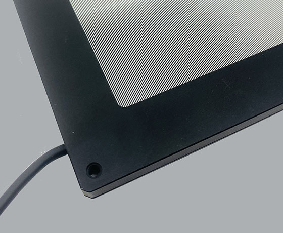
Principle:
This is a way to detect surface defects, such as bubbles, pits, scratches, etc., on mobile phone screens and screens of various electronic products. The traditional detection scheme is to use low angle light to detect, but in this way, the dirty dust on the sample surface will also cause interference with the defects. But by using the structure this interference can be ignored. By utilising the difference in depth of the defects, which is fed back into the stripes, even small defects become clear.
Features:
1. Scattered luminescence, good uniformity, clear imaging
2. Lightweight, thin thickness, easy to install, space-saving
3. Stripe interference imaging, used to detect bumps, cracks, ripples and other defects on smooth surfaces.
4. Stripe spacing of 0.6mm, 1mm and 2mm, suitable for different product testing, the surface using a special coating to reduce light interference.
Application:
1. Slightly reflective metal surface defect detection
2. Screen surface, optical film surface defect detection vertical wrinkle detection
3. Curved surface characters, feature detection
4. Electronic component pin detection
5. Bag surface printing content detection
6. Product colour difference detection